We are interested in engineering new ways to manipulate light, both on a chip and in free space. In our research, we exploit the mature nanofabrication technologies that have been developed by the semiconductor industry over the course of the last few decades, and use them to fabricate structures that are fractions the size of the wavelength of light. On this scale, we can “confuse” light into exhibiting unconventional properties such as anomalous refraction, chirality and enhanced nonlinear properties.
Since light is a substance that interacts with everything we care about, we can use these engineered properties to study a wealth of interdisciplinary topics, ranging from some that are obvious (fundamental physics, display technologies and laser sources) to others that might be unexpected (medical applications and quantum computation). Below we summarize some of our research directions, and provide links to relevant publications.
High-Q plasmonic metasurface resonators
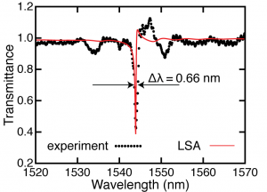
An optical resonator is one of the most fundamental tools in the science and technology of light, and is used to trap light to increase light-matter interactions for almost every application. It is highly desirable to maximize the quality factor of a resonator, as it will increase the efficiencies and reduce the footprints of many optical devices. We developed plasmonic metasurface nanoresonators with record-high Q-factors based on Surface Lattice Resonances (SLRs). Our platform therefore features the best of both worlds, incorporating the benefits of plasmonic materials (i.e., high local field enhancements, small footprint, and strong optical nonlinearities) with those of dielectric materials (i.e., long interaction times). Our group explores how to improve and expand the capabilities of SLRs for applications in filtering, active optical devices, and nonlinear optics.
Relevant publications
Epsilon-near-zero-enhanced nonlinear optics
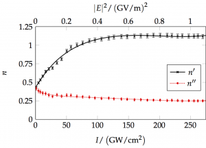
For as long as there have been optical materials, there has been an urgent demand for large optical nonlinearities. These could enable applications in all-optical computing, quantum optics and frequency-conversion, all on a wavelength scale. Epsilon-near-zero (ENZ) materials, such as indium tin oxide, have been found to exhibit record-breaking nonlinear optical responses and might be the key to unlocking these applications on a footprint that is comparable to electronic circuits. In our work, we study fundamental light-matter interactions within these materials and use nanostructures to exploit and enhance these enormous nonlinearities to demonstrate never-before-seen optical responses.
Relevant publications
Zero-index metamaterials
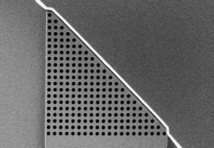 By creating sub-wavelength structures, we can trick light into demonstrating properties that are not present in its constituent materials. These kinds of structures, called metamaterials, can even be designed to exhibit material responses that do not appear in nature, such as magnetic responses at optical frequencies, extremely small or negative indices of refraction, and tunable optical activity. In our work, we exploit the ubiquity and fabrication precision of silicon photonics to demonstrate multiple platforms of all-dielectric integrated metamaterials with a refractive index near zero. A flexible integrated zero-index metamaterial enables many applications, including in quantum optics, interconnects and wavefront engineering.
Relevant publications
Titanium dioxide photonics
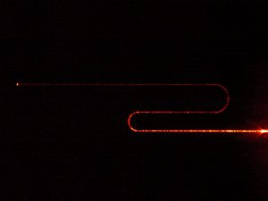
Though silicon is cheap, abundant, nontoxic, and already has established fabrication capabilities bolstered by the semiconductor industry, it suffers from many unfavorable properties, such as being opaque to visible wavelengths and multi-photon absorption. By contrast, titanium dioxide (TiO2) is completely transparent down to a wavelength of 400 nm and does not suffer from two- or even three-photon absorption in the telecom regime. It boasts the largest linear and nonlinear coefficients for a material with these properties, and it too is an abundant, non-toxic semiconductor. These features make TiO2 a promising platform for integrated nonlinear devices. In addition, it possesses a host of unique photocatalytic and self-cleaning properties, as well as a negative thermo-optic coefficient, a trait that enables entirely passive temperature compensation. Our team pioneered the nanofabrication process for titanium dioxide photonics, developing everything from thin-film deposition to the structuring procedure.